- 您现在的位置:买卖IC网 > Sheet目录3875 > PIC16F628A-I/P (Microchip Technology)IC MCU FLASH 2KX14 EEPROM 18DIP
PIC16F627A/628A/648A
DS40044G-page 142
2009 Microchip Technology Inc.
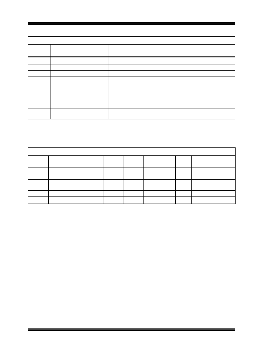
TABLE 17-2:
COMPARATOR SPECIFICATIONS
TABLE 17-3:
VOLTAGE REFERENCE SPECIFICATIONS
Operating Conditions: 2.0V
< VDD <5.5V, -40°C < TA < +125°C, unless otherwise stated.
Param
No.
Characteristics
Sym
Min
Typ
Max
Units
Comments
D300
Input Offset Voltage
VIOFF
—
±5.0
±10
mV
D301
Input Common Mode Voltage
VICM
0—
VDD – 1.5*
V
D302
Common Mode Rejection Ratio
CMRR
55*
—
db
D303
Response Time(1)
TRESP
—
300
400
400*
600*
ns
VDD = 3.0V to 5.5V
-40° to +85°C
VDD = 3.0V to 5.5V
-85° to +125°C
VDD = 2.0V to 3.0V
-40° to +85°C
D304
Comparator Mode Change to
Output Valid
TMC2OV
—300
10*
μ
s
* These parameters are characterized but not tested.
Note 1:
Response time measured with one comparator input at (VDD – 1.5)/2, while the other input transitions from
VSS to VDD.
Operating Conditions: 2.0V < VDD < 5.5V, -40
°C < TA < +125°C, unless otherwise stated.
Spec
No.
Characteristics
Sym
Min
Typ
Max
Units
Comments
D310
Resolution
VRES
——
VDD/24
VDD/32
LSb
Low Range (VRR = 1)
High Range (VRR = 0)
D311
Absolute Accuracy
VRAA
—
1/4(2)*
1/2(2)*
LSb
Low Range (VRR = 1)
High Range (VRR = 0)
D312
Unit Resistor Value (R)
VRUR
—2k*
—
Ω
D313
Settling Time(1)
TSET
——
10*
μ
s
* These parameters are characterized but not tested.
Note 1:
Settling time measured while VRR = 1 and VR<3:0> transitions from ‘0000’ to ‘1111’.
2:
When VDD is between 2.0V and 3.0V, the VREF output voltage levels on RA2 described by the
equation:[VDD/2 ± (3 – VDD)/2] may cause the Absolute Accuracy (VRAA) of the VREF output signal on RA2
to be greater than the stated max.
发布紧急采购,3分钟左右您将得到回复。
相关PDF资料
PIC18F24K22-I/SO
IC PIC MCU 16KB FLASH 28SOIC
PIC18F23K22-I/SP
IC PIC MCU 8KB FLASH 28SPDIP
PIC18LF23K22-I/SP
IC PIC MCU 8KB FLASH 28SPDIP
PIC24F08KA102-I/SS
IC PIC MCU FLASH 8K 28-SSOP
PIC16C58B-20/SO
IC MCU OTP 2KX12 18SOIC
PIC12C672-04/SM
IC MCU OTP 2KX14 A/D 8-SOIJ
PIC18F25K20-E/SS
IC PIC MCU FLASH 16KX16 28-SSOP
PIC18F25J10T-I/SO
IC PIC MCU FLASH 16KX16 28SOIC
相关代理商/技术参数
PIC16F628A-I/P
制造商:Microchip Technology Inc 功能描述:IC 8BIT FLASH MCU 16F628 DIP18
PIC16F628A-I/SO
功能描述:8位微控制器 -MCU 3.5KB 224 RAM 16 I/O RoHS:否 制造商:Silicon Labs 核心:8051 处理器系列:C8051F39x 数据总线宽度:8 bit 最大时钟频率:50 MHz 程序存储器大小:16 KB 数据 RAM 大小:1 KB 片上 ADC:Yes 工作电源电压:1.8 V to 3.6 V 工作温度范围:- 40 C to + 105 C 封装 / 箱体:QFN-20 安装风格:SMD/SMT
PIC16F628A-I/SO
制造商:Microchip Technology Inc 功能描述:8BIT FLASH MCU SMD 16F628 SOIC18
PIC16F628A-I/SOG
制造商:Microchip Technology 功能描述:MCU 8-Bit PIC16 PIC RISC 3.5KB Flash 3.3V/5V 18-Pin SOIC W Tube
PIC16F628A-I/SS
功能描述:8位微控制器 -MCU 3.5KB 224 RAM 16 I/O RoHS:否 制造商:Silicon Labs 核心:8051 处理器系列:C8051F39x 数据总线宽度:8 bit 最大时钟频率:50 MHz 程序存储器大小:16 KB 数据 RAM 大小:1 KB 片上 ADC:Yes 工作电源电压:1.8 V to 3.6 V 工作温度范围:- 40 C to + 105 C 封装 / 箱体:QFN-20 安装风格:SMD/SMT
PIC16F628A-I/SS
制造商:Microchip Technology Inc 功能描述:8BIT FLASH MCU SMD 16F628 SSOP20
PIC16F628AT-E/ML
功能描述:8位微控制器 -MCU 28LD 20MHz 2K FLASH RoHS:否 制造商:Silicon Labs 核心:8051 处理器系列:C8051F39x 数据总线宽度:8 bit 最大时钟频率:50 MHz 程序存储器大小:16 KB 数据 RAM 大小:1 KB 片上 ADC:Yes 工作电源电压:1.8 V to 3.6 V 工作温度范围:- 40 C to + 105 C 封装 / 箱体:QFN-20 安装风格:SMD/SMT
PIC16F628AT-E/SO
功能描述:8位微控制器 -MCU 18LD 20MHz 2K FLASH RoHS:否 制造商:Silicon Labs 核心:8051 处理器系列:C8051F39x 数据总线宽度:8 bit 最大时钟频率:50 MHz 程序存储器大小:16 KB 数据 RAM 大小:1 KB 片上 ADC:Yes 工作电源电压:1.8 V to 3.6 V 工作温度范围:- 40 C to + 105 C 封装 / 箱体:QFN-20 安装风格:SMD/SMT